Interface Specification
Port list (qspi_top)
Clock/reset
Signal |
Direction |
Width |
Description |
|---|---|---|---|
|
in |
1 |
system clock (all logic, including SCK generation) |
|
in |
1 |
asynchronous reset, active low |
OBI subordinate ports
Two identical OBI ports (types spi_obi_req_t/spi_obi_rsp_t from
spi_pkg.sv, 32-bit address/data, 4-bit ID):
Port |
Window (hatch) |
Function |
|---|---|---|
|
|
registers (indirect mode) |
|
|
memory-mapped window |
Serial side (QSPI)
Signal |
Direction |
Width |
Description |
|---|---|---|---|
|
out |
1 |
chip select, active low |
|
out |
1 |
serial clock, mode 0 (idles low), max. |
|
out |
4 |
drive values of lanes SIO0…3 |
|
out |
4 |
output enable per lane (1 = drive) |
|
in |
4 |
sampled lane values |
Lane assignment: single-SPI transmits on SIO0 (MOSI) and receives on SIO1
(MISO); dual uses SIO1:0, quad SIO3:0 (MSB on the highest lane). The
tri-state belongs at the pad/chip top:
assign pad[i] = oe[i] ? o[i] : 1'bz;.
OBI protocol (subset used)
Single-beat OBI: request channel with req/gnt, response channel with
rvalid (no rready — the response is valid for exactly one cycle). gnt
is combinational; a transfer happens on every clock edge with req && gnt.
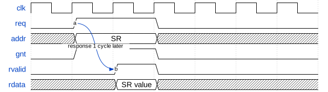
The CSR port responds in the following cycle; DR accesses may delay gnt by
one cycle (FIFO hazard, see below). The MEM port withholds gnt while a
transaction is in flight (single outstanding) and responds after the
transfer ends — on errors (FSIZE, mmap off, WCCR.DMODE=0) with err=1.
CSR read (response one cycle later):
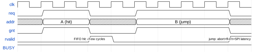
mmap read with prefetch hit vs. demand read (schematic):
Byte enables: reads always return the full word (be ignored); writes
evaluate be — the MEM port only accepts contiguous patterns
(sb/sh/sw), otherwise err. At the DR register, be selects the
transfer width (1/2/4 bytes).
SPI timing (mode 0)
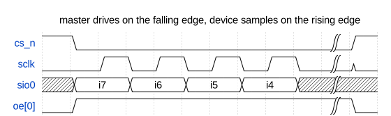
The controller drives outputs on the falling and samples inputs on the
rising SCK edge; the device mirrors this. SCK idles low (CKMODE=0).
CS goes low half an SCK period before the first edge and high again after
the last edge; DCR.CSHT then enforces a minimum CS-high time.
Single-SPI frame, instruction phase (MSB first):
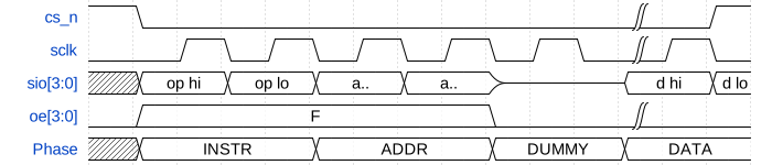
SQI read (23LC1024 profile): instruction + address quad from the master, then 2 dummy clocks (bus turnaround, all lanes high-Z), then data quad from the device:
SCK may pause between two bytes (CS stays low) — static SPI slaves only react to edges. The controller uses this for FIFO backpressure and TX-underrun stalls; visible on the bus as SCK gaps within a frame. This is protocol-legal for both target chips.
Configuration limits
Parameter |
Value |
Note |
|---|---|---|
SCK |
|
one clock domain, no CDC |
FIFO |
32 bytes (parameter |
doubles as prefetch buffer |
Address space |
|
FSIZE limits effectively |
Dummy |
0–31 SCK clocks ( |
|
Address |
1–4 bytes ( |
both target chips: 3 |