Access to modern integrated circuit design education is often limited by the availability of proprietary tools and the complexity of industrial design flows. As a result, students rarely have the opportunity to experience the full process from RTL to a fabrication-ready design within an academic setting. In recent years, open-source EDA tools have started to change this landscape, enabling more accessible and reproducible design workflows.
Design your Chip was created as a response to this shift: a course designed to bring the complete chip design experience into the classroom using a fully open-source toolchain. Rather than focusing on isolated concepts, the course guides students through the entire RTL-to-GDS flow while working on their own projects.
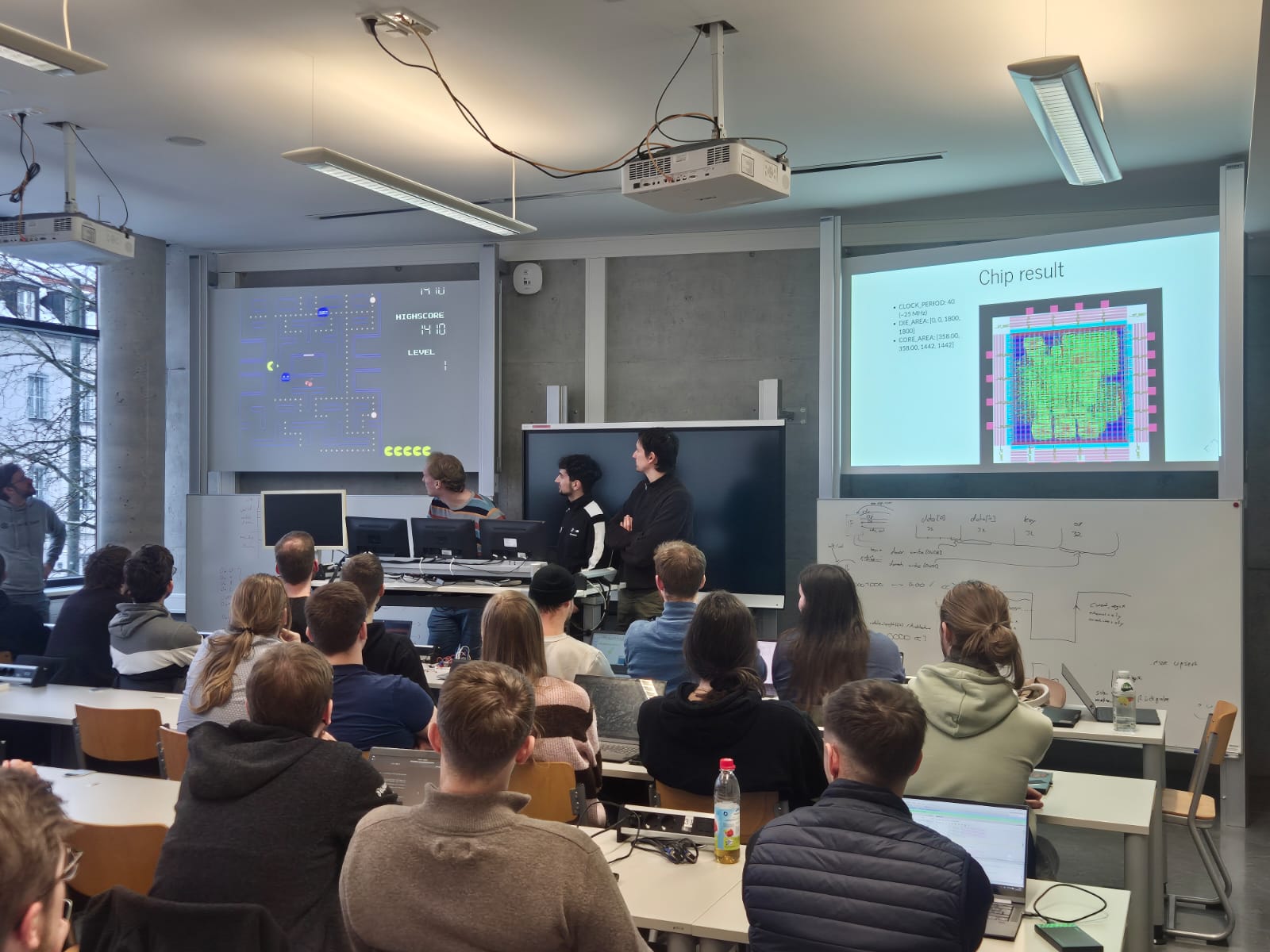
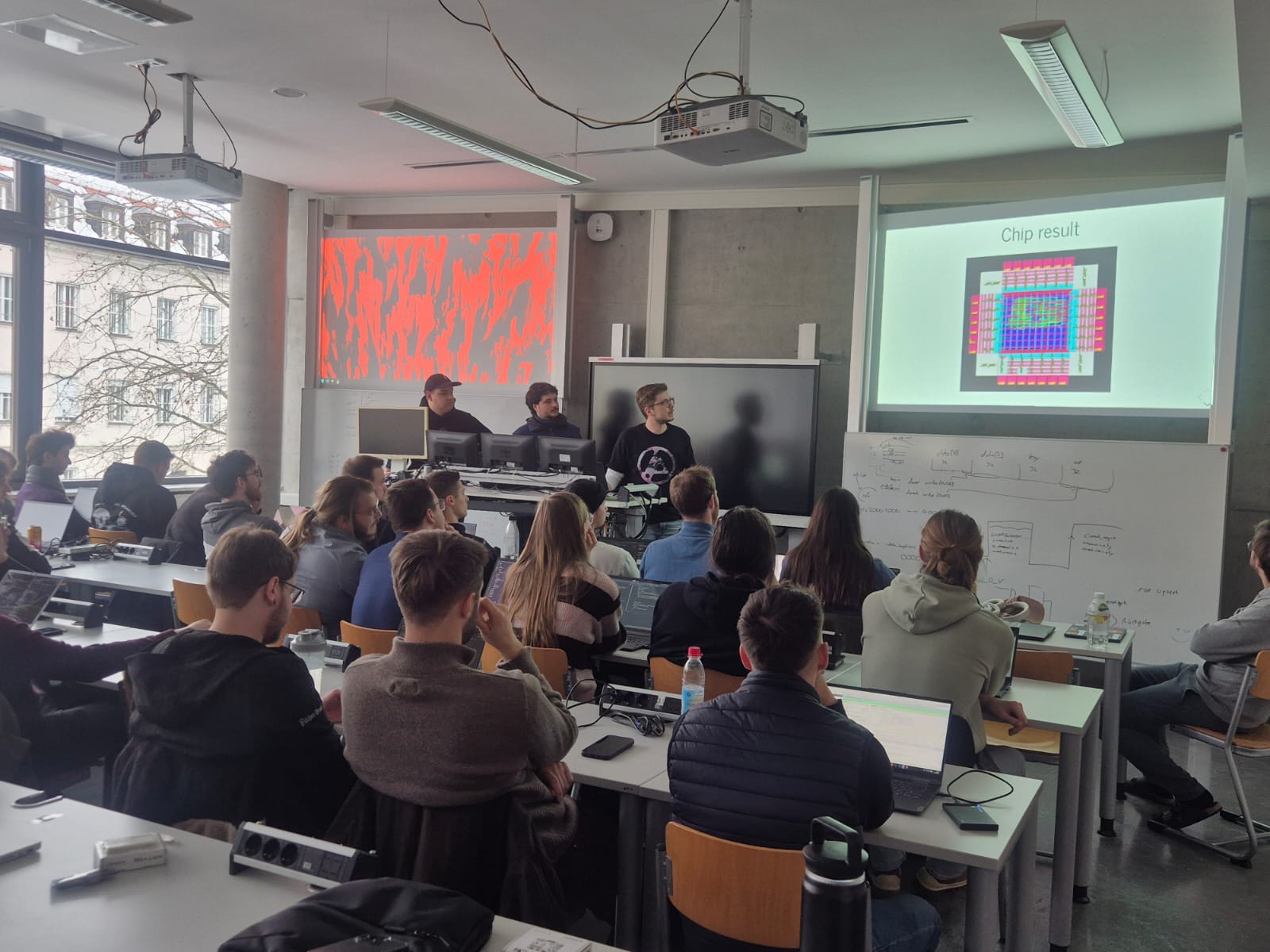
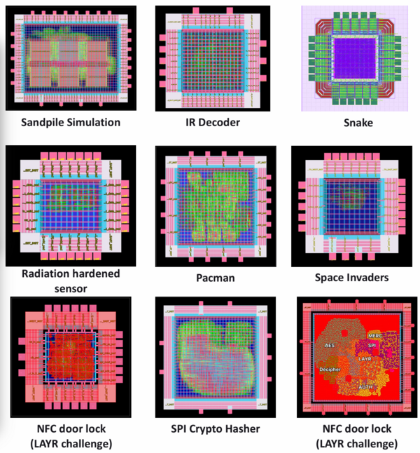
As part of this approach, students developed a wide range of projects. The diversity of these projects reflects both the flexibility of the flow and the creativity of the participants. Some teams developed game-oriented designs such as Pac-Man and Space Invaders, while others focused on more specialized topics. Several groups worked on encryption and hardware security systems, one team explored radiation hardening techniques, and another focused on image processing. This range of projects highlights how the same design framework can be applied across very different application domains.
This course was organized by the AEMY research group and represents an important step in its ongoing effort to promote open-source IC design education. Previous initiatives include the ChipUSM Summer Camp in Chile at the end of 2025 and the recent POEMS Spring School 2026 in Portugal. This time, however, we were hosting the course locally, which allowed us to take it a step further: offering it as an official credited course and providing students with a real opportunity to reach tapeout using an open-source technology.
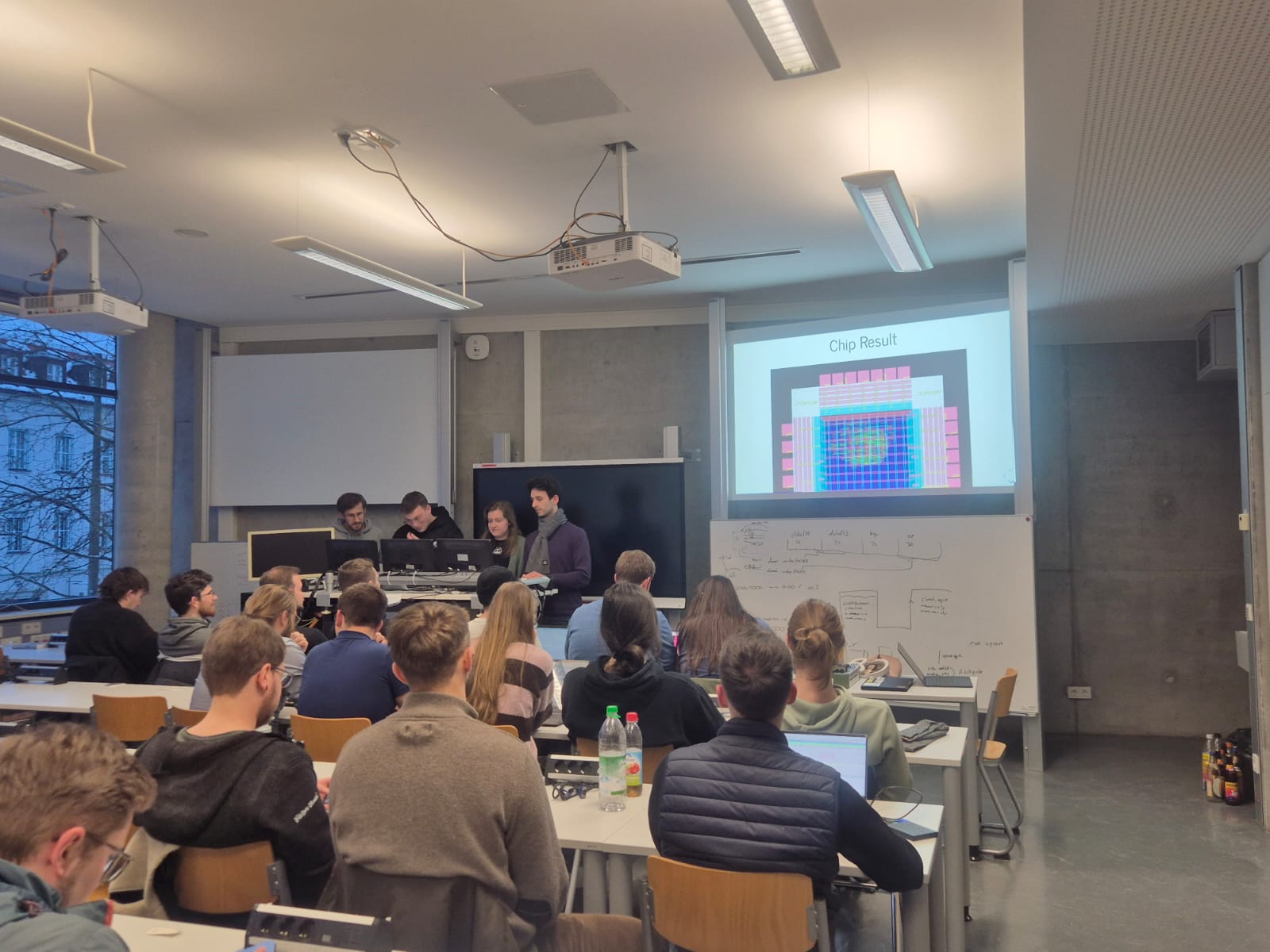
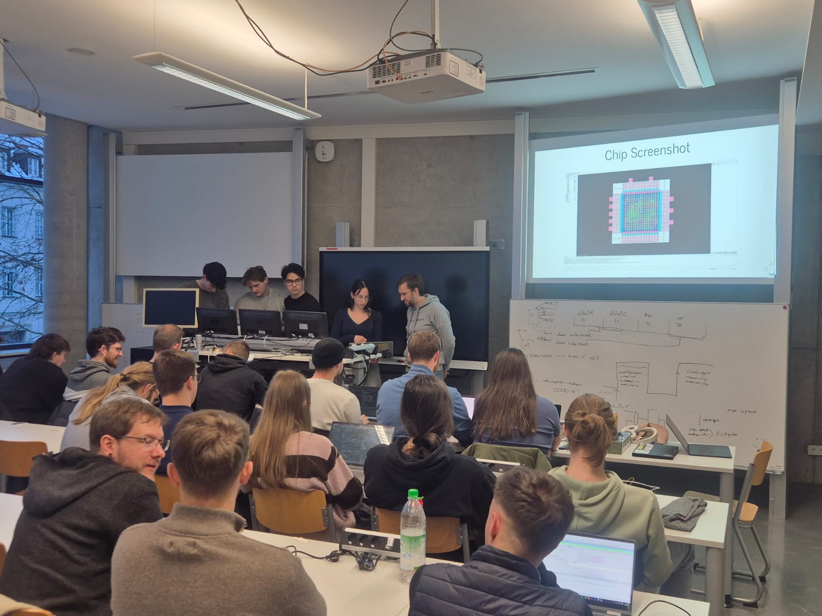
In practice, the course was held over two weeks of full-time work, from February 9 to 20, at Hochschule München. It brought together 76 undergraduate and master’s students interested in modern digital IC design with open-source tools. During the course, 15 working groups were formed. The main objective was for each team to reach a fabrication-ready GDS. Out of these, 14 groups successfully achieved this goal. Notably, 5 of them went further and were submitted for tapeout by the end of March using the IHP SG13G2 technology.
Course structure and content
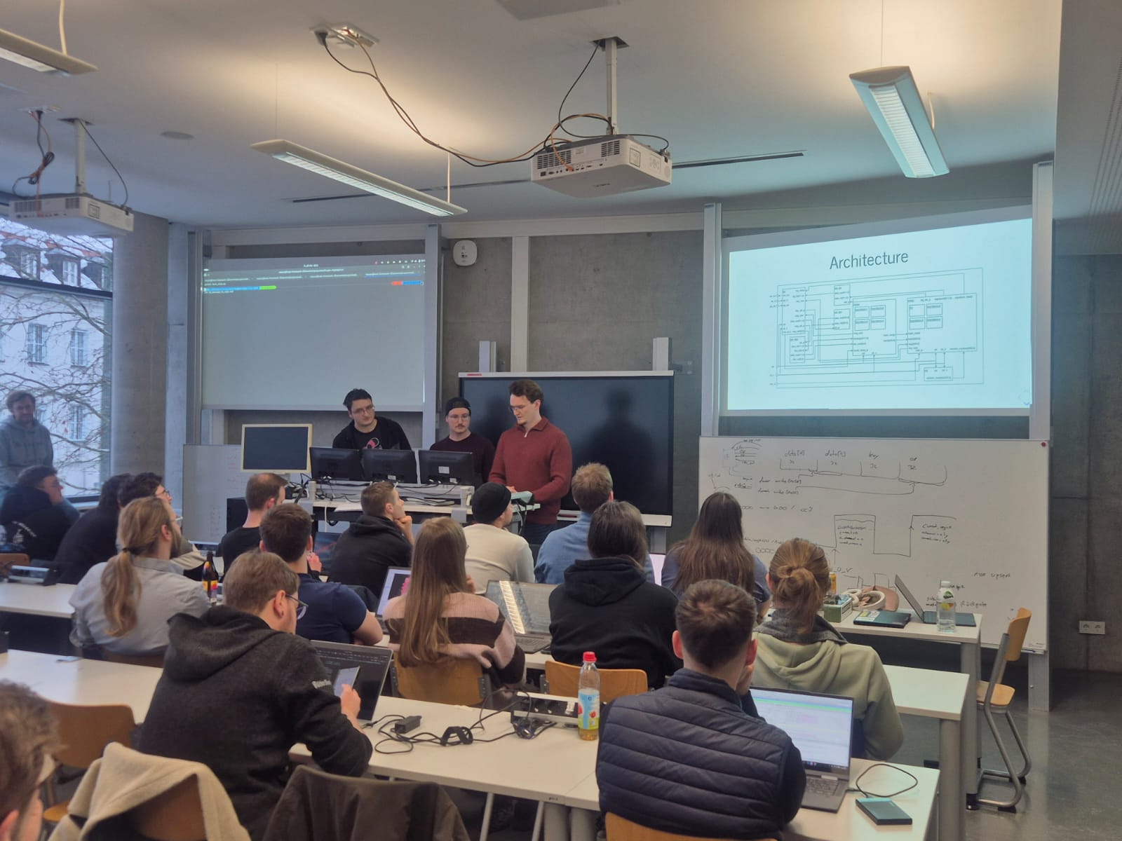
The course was structured around the complete digital design flow, guiding students from RTL design to a fabrication-ready GDS. Rather than treating each step in isolation, the flow was presented as a continuous process, allowing participants to understand how design decisions propagate across different stages.
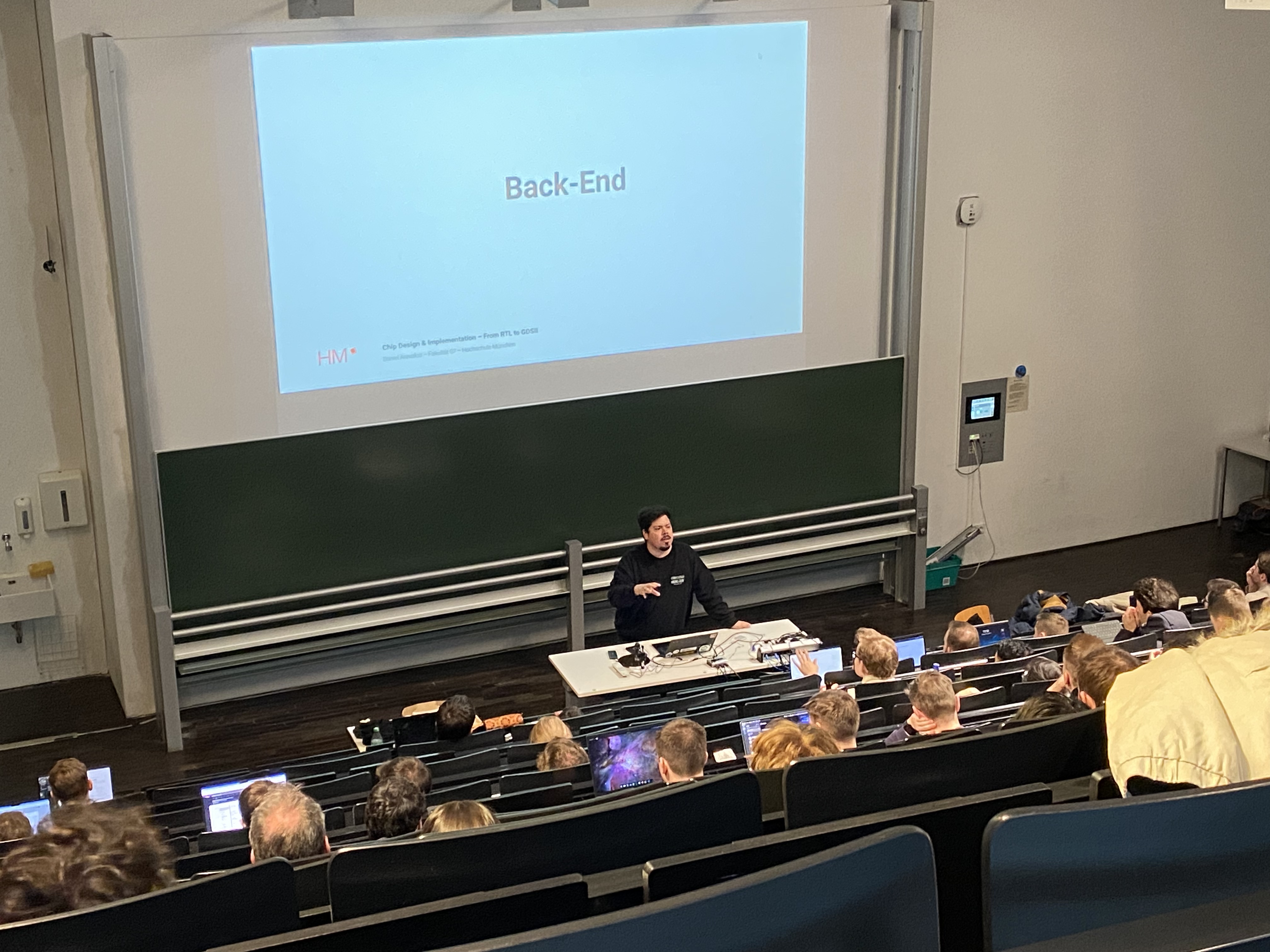
The first day began with a series of lecture-style sessions, introducing the broader context of microelectronics in Europe and the world as well as the overall design and fabrication process. This was followed by an overview of the RTL-to-GDS flow, including a full demonstration of the toolchain.
At the end of the first day and throughout the second day, students participated in a guided “first chip” activity. This combined hands-on guidance with individual work, allowing participants to interact with the tools for the first time and produce a simple but functional chip design.
During these initial days, students were also organized into groups and asked to define their own project, either based on proposals from the tutors or their own ideas, which they would develop throughout the course.
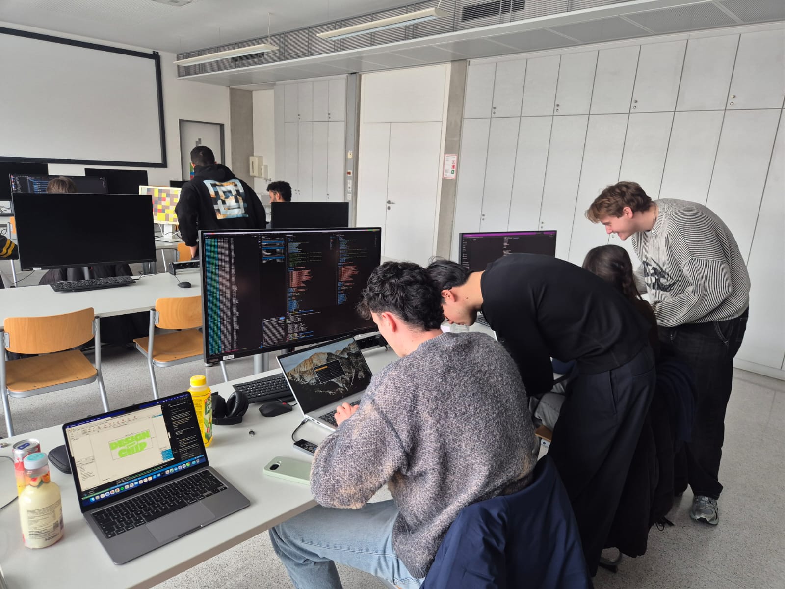
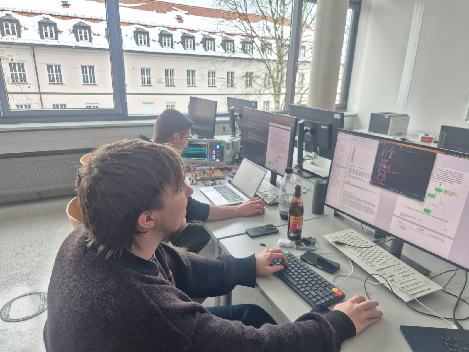
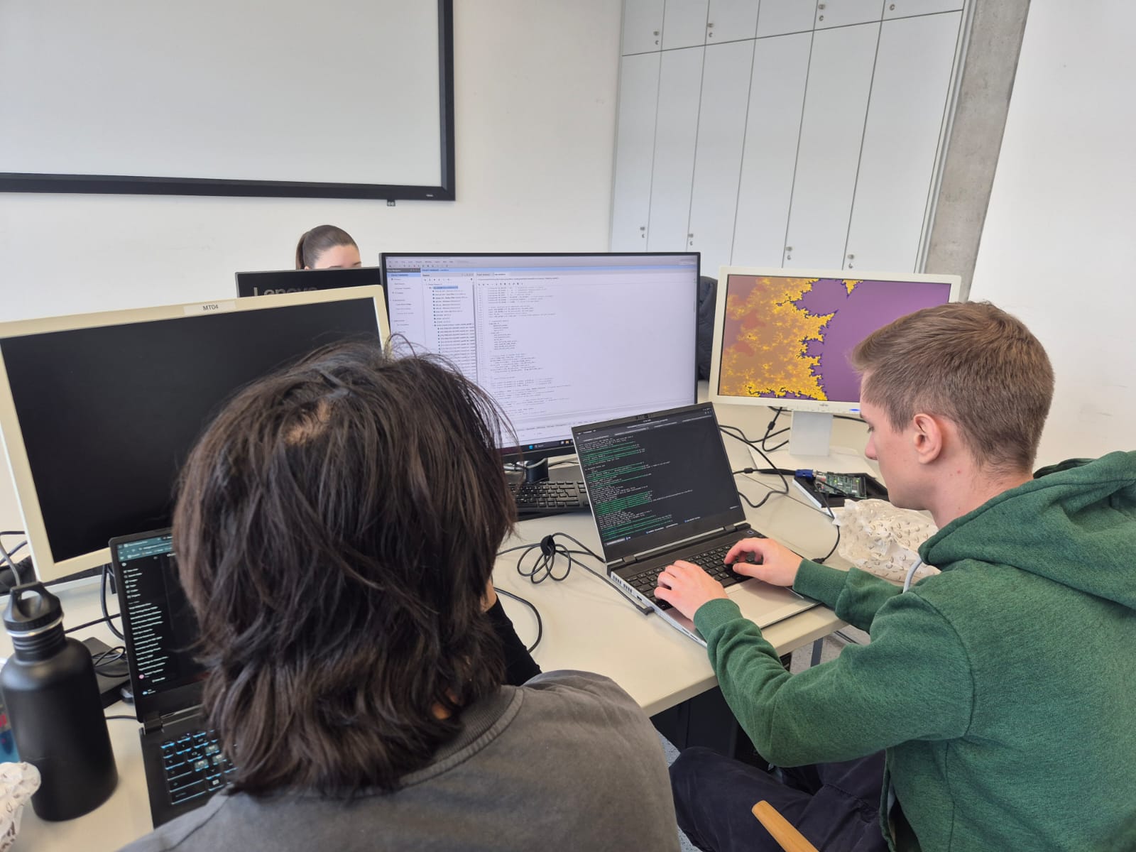
From the third day onwards, students worked in dedicated rooms in their teams, with regular support from the AEMY tutors. The work was structured around clearly defined milestones, including design development, FPGA-based testing, and physical implementation. Progress was tracked through an intermediate presentation at the end of the first week and a final presentation at the end of the course.
Metodology
The course was designed around an active, project-driven learning approach, where students were encouraged to take ownership of their work from an early stage. Rather than following step-by-step instructions, participants were guided to make their own design decisions, explore trade-offs, and iterate on their solutions throughout the process.
A key aspect of the methodology was the use of team-based projects with clearly defined milestones. This structure allowed students to progressively validate their designs, from functional verification and FPGA-based testing to physical implementation. The emphasis was placed on autonomy and iterative development, with tutors providing guidance while allowing teams to take ownership of their projects.
Results and conclusions
The results of the course highlight the effectiveness of a hands-on, end-to-end approach to teaching digital IC design. Within just two weeks, most teams were able to progress from initial concepts to fabrication-ready designs, demonstrating how quickly students can engage with the complete design flow when provided with the right tools and structure.
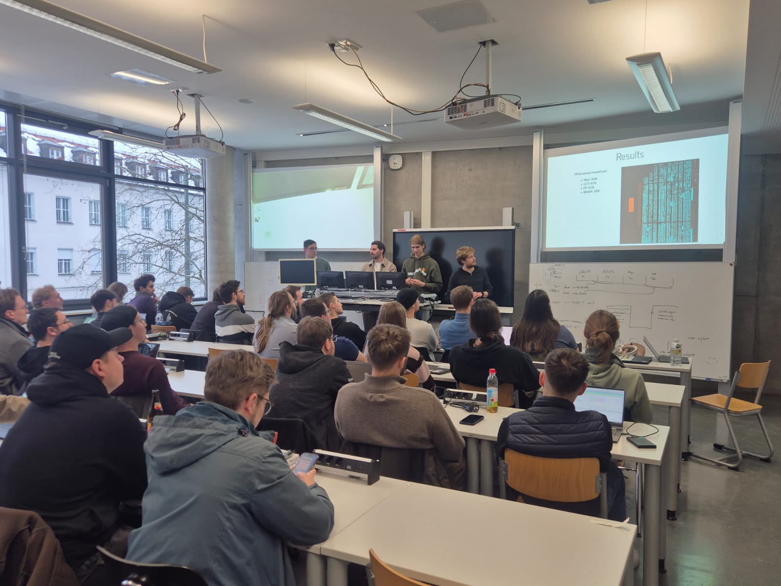
Beyond reaching a GDS, all groups validated their designs through FPGA-based testing, reinforcing the importance of functional verification before physical implementation. This progression allowed students to experience not only the design process itself, but also the iterative nature of hardware development.
A key factor behind these results was the decision to let students define their own projects. This approach encouraged creativity, allowed participants to build on their own interests or previous experience, and naturally led to the formation of teams around shared goals. As a result, students were more engaged and able to take stronger ownership of their work throughout the course.
Building on these results, five projects went even further and were submitted for tapeout using the IHP SG13G2 technology. Achieving this within such a short timeframe represents a significant milestone in an academic context, bringing student-developed designs into a real fabrication process.